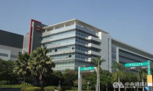
TSMC to hold 3nm process mass production launch ceremony on Dec. 29
12/24/2022

Taipei, Dec. 24 (CNA) Taiwan Semiconductor Manufacturing Co. (TSMC), the world’s largest contract chipmaker, on Saturday announced it will hold a ceremony on Dec. 29 to celebrate the start of mass production using its 3 nanometer process and plans for further expansion of the technology in southern Taiwan.
At the ceremony, TSMC will celebrate the placing of the last beam at the new facility — an event known as a “topping out” — for the launch of the 3nm process at Fab 18 located in the Southern Taiwan Science Park, Tainan. It will also detail plans to further expand 3nm production at the facility in the coming years. Currently, TSMC mass produces chips made using the 5nm process at Fab 18.
It is unusual for TSMC to hold a ceremony to mark the beginning of commercial production of a new technology. Market analysts speculate that the company is holding the ceremony to publicize its intention to keep using Taiwan as a hub for research, development and production, despite its overseas investments.
Suspicion has risen that TSMC could relocate its production and R&D efforts to the United States after the chipmaker said at a first tool-in ceremony for a 12-inch wafer plant in the U.S. state of Arizona on Dec. 6 that it would increase its planned US$12 billion investment in Arizona to US$40 billion to build not only a 4-nanometer fab scheduled to begin production in 2024 but also a 3nm fab scheduled to begin operations in 2026.
Those concerns have intensified since TSMC sent a large group of engineers from Taiwan to support the Arizona plant, prompting many investors to fear that the chipmaker’s base in Taiwan could lose its advantage by escalating competition on the global market through its move overseas.
The two phases of investment in both 4nm and 3nm processes in Arizona are expected to produce more than 600,000 wafers a year, according to TSMC.
Last week, TSMC CEO C.C. Wei (魏哲家) said at a forum held by Mount Jade Global Science and Technology Association in Taipei, that there is “no chance” building a wafer fab in one place will give it a technical advantage over other semiconductor manufacturing sites, referring to the Arizona plant and the expansion plan in the U.S. state.
After launching mass production of the 3nm process, the technology will become the latest used by TSMC for commercial production. Next year, the company is scheduled to mass produce the N3E process, which is based on 3nm technology and will produce more efficient chips with a better yield rate.
TSMC is also developing the more sophisticated 2nm process and will build a 2nm fab in Hsinchu with mass production scheduled to begin in 2025.
The 3nm process uses 16nm FinField-effect-transistor (FinFET) technology, which is a 3D transistor structure that allows a chip to run faster using the same amount of power or to run at the same speed on reduced power. Compared with the 5nm process, which started mass production last year, it will raise speeds by 10-15 percent and be 25-30 percent more efficient in energy use.
International brands such as Apple Inc. and Intel Corp. are expected to place orders for TSMC’s 3nm process, analysts said.
Moreover, the 2nm process will be the first technology in which TSMC employs a Gate-All-Around (GAA) structure, which reduces undesirable variability and mobility loss, making the technology the most competitive and efficient on the market.
In early December, Wayne Wang (王永壯), director general of the Hsinchu Science Park Bureau, said TSMC has plans to build a 1nm process fab in the Longtan section of Hsinchu Science Park, a statement the chipmaker has not confirmed.
Source:TSMC to hold 3nm process mass production launch ceremony on Dec. 29 – Focus Taiwan

