NVIDIA’s Spectrum-X Ethernet Photonics Debuts as the World’s First 200G Co-Packaged Optics, Supercharging the Future of AI
Aug 26, 2025
NVIDIA’s silicon photonics interconnect technology is expected to replace the traditional optical interconnect, and Spectrum-X Ethernet Photonics’ rundown shows how big a role it will play in scaling AI compute.
NVIDIA’s Photonics Bring In a Whopping 3.5X Increase in Power Efficiency, Catering to Limitations of Optical Connections
When the industry talks about silicon photonics, the implementation is more focused on D2D interconnects and how hardware manufacturers like AMD or Intel will use it; however, NVIDIA has other plans.

In a detailed rundown at Hot Chips 2025, NVIDIA presented its next-gen Spectrum-X Ethernet Photonics interconnect, which features massive improvements when it comes to scaling AI factories, and more importantly, ensuring that implementation leads to an effective replacement of the traditional optical interconnect.

NVIDIA initially discusses the need for co-packaged photonics and how drastically it benefits scaling AI factories. The firm mentions that an AI factory consumes around 17 times more optics power relative to a traditional cloud data center, mainly because the increase in GPU clusters requires dozens of optical transceivers to talk to other GPUs. Due to this, network optics alone cost around 10% of the total compute power of an AI factory, which is a huge number that NVIDIA plans to reduce through Spectrum-X Ethernet Photonics.

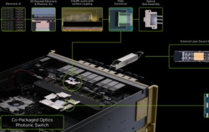
Spectrum-X Ethernet Photonics is a unique implementation that is claimed to be the first to feature 200 G/lane SerDes, the cutting-edge standard in electrical signaling. Compared to pluggable transceivers, Spectrum-X photonics features better signal integrity and lower DSP requirements since, in this implementation, the photonic engine (PIC) is right next to the switch ASIC. This means no long PCB traces and a drastic decrease in laser count. For example, a 1.6 Tb/s link drops to just two lasers from eight, which means lower power consumption and higher transfer reliability.

NVIDIA’s silicon photonics solution features a Silicon Photonics CPO chip with an ultra-high 1.6T transfer. With MRMs (Micro-Ring Modulators) onboard, the solution offers much higher bandwidth with lower power and footprint. More importantly, NVIDIA Photonics is the first to feature 3D stacking between the photonic and electronic layers, reducing routing complexity and increasing bandwidth density. Team Green partnered up with TSMC on silicon photonics since the Taiwan giant is the go-to spot for your photonics needs.

NVIDIA photonics, employed in a data center, is claimed to feature 3.5x higher power efficiency, 10x higher resiliency, and 1.3× faster time to operation relative to the optical standard, and this shows that AI compute will scale tremendously once photonics becomes the mainstream interconnect. The firm also showcased its first full-scale switch with integrated photonics, the Spectrum-6 102T, which will be the flagship offering from Team Green. Here’s what it will .
If I summarize the above technical in a few words, NVIDIA Photonics is intended to reduce power consumption, ensure easier scaling, and, more importantly, speed up the interconnect process by leveraging the power of photons. Co-packaged silicon optics support 3x higher GPU under ISO power and ~4× reduction in total lasers, which means a huge chunk of your power is shifted away from networks to the actual GPU clusters onboard, leading to improved performance.